Laser Marking
Silicon Connection provide in-house Laser Marking Services for our wafer handling products.
Laser Marking is one of our in-house services that we provide for our clients in the semiconductor or other related industries. The laser marking is commonly requested by our regular client to be done on PFA (Perfluoroalkoxy alkanes) / PEEK (Polyether ether ketone) / PP (Polypropylene) material of wafer cassettes or storage boxes.
Laser Marking is a cleaner option for marking identification such as serial number or bar code onto the material, through this process no residue or substance will come off from the marking. This is the ideal marking method as most wafer fabs are sensitive to outgassing and particles from alternative labelling method such as laminating labels, card holders or hot stamping. As technology advances, laser marking will soon become a standard in the high-tech industries.
We are licensed to carry out laser marking in our facility and our team members are licensed to carry out laser marking for our clients, complying to NEA guideline. Our team members are highly experienced in carrying out laser marking according to our clients’ requirement.
Other than the mentioned materials, occasionally Silicon Connection receives request to laser mark stainless steel wafer ring frame, graphite and SiC (Silicon Carbide) materials, including graphite crucibles and other fab critical materials.
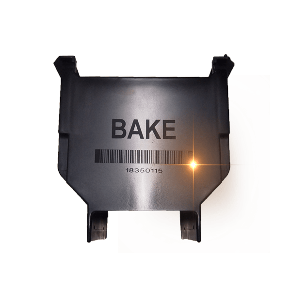
The laser marking expenses will vary depending on the complexity and size of the marking, according to alphanumeric characters or barcode (as shown in the picture). Designs and specifications can be customised according to your products and requirements.
Contact Us today if you have a laser marking request and we will be happy to assist you.
Looking for services or support?
Let us know your technical enquiries and we will try our best to help you.