Technology is quickly shifting to a higher overall percentage of thinner and more sensitive wafers. The main driver behind the thinner, more sensitive wafers is the consumer electronics industries need for smaller, higher performing and lower cost device configurations.
These devices are used in advanced chip designs for 3D, 2.5D, SOC, MEMS, LED and power semiconductors. These new requirements along with 3D applications, are pushing demand for more thin and ultrathin, lens or bumped semiconductor wafers.
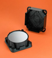
As wafer thickness decrease, manufacturing challenges arise. Ultrathin wafers are less stable and more vulnerable to stresses, and the die can be prone to breaking and warping. Entegris new 200 mm contactless shipper helps address shipping requirements.
Feel free to contact us for more details.