NBS Semiconductor
NBS Semiconductor leads in the global arena of wafer handling and inspection equipment. NBS advanced systems facilitates automatic inspection of imperfections such as silicon micro cracks and peripheral breakages, to make wafer handling a highly secure process.
NBS expertise in the area of wafer packing is allowing us to continuously develop new solutions for the Semiconductor industry. NBS creates systems that are compliant with the SEMI* standard in accordance to industry requirements.
NBS Products
NBS Semiconductor has the technical expertise and skills in the wafer packing and sorting.
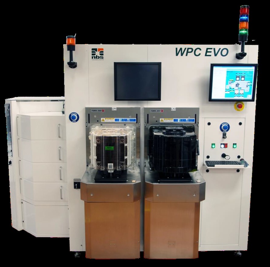
We offer wafer handling solutions for wafer sizes 150mm, 200mm & 300mm, including thinned wafers.
Our experienced Engineers are here to support your operations.
Our tool is SEMI SECSII/ GEM/ 300mm software compliant with user friendly GUI.
Read more about our NBS WPC EVO here.
Read more about NBS here.
Please contact us for more information.
Looking for Wafer Handling Equipment?
Check out the functionalities and video of NBS Wafer Packing Equipment.